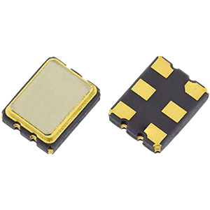
GVXO-L33L
3.3V Complementary LVDS VCXO with Low Phase Jitter
- Complementary LVDS outputs
- Multiplier-free design
- Enable / disable tristate function
- Designed for high speed data transfer
Specifications
| Frequency range |
40.0 ~ 250MHz |
| Dimensions |
3.2 x 2.5 x 1.1mm |
| Voltage control (VCTL) |
+1.65V ±1.50V, 10% linearity |
| Storage temperature range |
-40 to +85°C |
| Supply voltage (VDD) |
+3.3V (±5%) |
| Supply current |
25mA max |
| Output |
LVDS |
| Offset voltage |
1.25V typ |
| Differential output voltage |
0.35V typ |
| Waveform symmetry |
45:55 max @ 50%VP-P |
| Rise / fall time |
0.4ns max (20% ~ 80%VP-P) |
| Phase jitter |
1ps max (12kHz ~ 20MHz) |
| Enable / disable function |
Tristate (control via pad 2) |
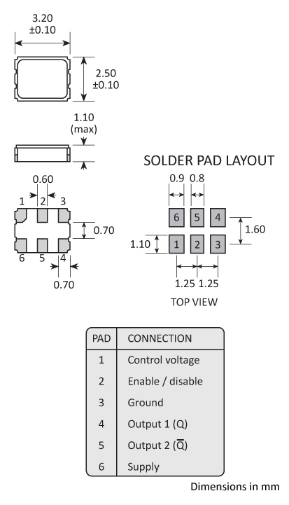
Package Drawing

Ordering Information
To request a quotation for the GVXO-L33L please use the configurable options form to choose the options you require and then submit your configured product to our team. Our expert advisers are always happy to help with your requirements and can be contacted on +44 1460 256 100 or at sales@golledge.com.
Once we've received your request our expert team will then produce a quotation tailored to meet your needs using the option codes you've selected.
Following product selection you will be issued with a seven character Golledge part number. Your Golledge part number is the internationally accepted Golledge manufacturing part number (MPN) that should be used for all project documentation, including bills of materials (BoMs) and purchase orders.
If you have any queries regarding any of our documentation our dedicated sales team will be happy to help.
Enable / Disable Function
| Input (pad 2) | Output 1 (pad 4) | Output 2 (pad 5) |
|---|---|---|
| Open | Enabled | Enabled |
| '1' level (≥0.7 VDD) | Enabled | Enabled |
| '0' level (≤0.3 VDD) | High Impedance | High Impedance |
Marking


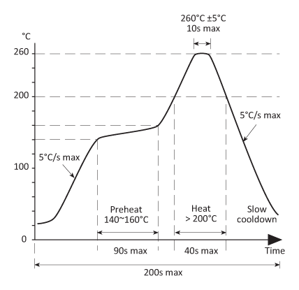
Soldering Profile

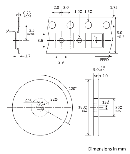
Tape & Reel Specification

Handling & Storage
 Human Body Model (HBM) 1A (250V to <500V)
 Moisture Sensitivity Level (MSL): 1 (or not applicable)
Construction
Ceramic body with gold-plated pads. Metal lid, seam sealed
Compliance
 Lead-free (< 0.1% by weight )
 RoHS compliant with no exemptions. See our declaration
 REACH compliant. See our statement
 Free of conflict minerals. See our declaration
 Free of Halogens. See our declaration
 Free of Ozone-depleting substances. See our declaration
