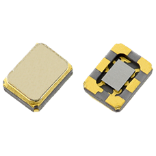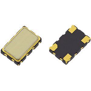
GTXO-83V
2.4V ~ 3.6V SM VCTCXO with Clipped Sine Output
- Low power consumption
- Supply voltage from 2.4V ~ 3.6V
- Miniature SM package
- Excellent frequency stability
Specifications
| Frequency range |
9.5 ~ 45.0MHz |
| Dimensions |
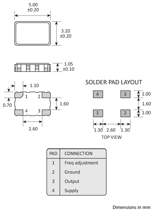
5.0 x 3.2 x 1.15mm |
| Storage temperature range |
-40 to +85°C |
| Supply voltage stability |
±0.2ppm, VDD ±5% |
| Load stability |
±0.2ppm, ZL ±10% |
| Ageing |
±1.0ppm max first year |
|
Supply voltage (VDD)
* see note below |
+2.4V ~ +3.6V |
| Supply current |
1.5mA max (9.5 ~ 20.0MHz) 2.0mA max (20.0 ~ 32.0MHz) 2.5mA max (32.0 ~ 45.0MHz) |
| Output waveform |
Clipped sine, 0.8V p-p, +DC offset |
| Test load (ZL) |
10kΩ // 10pF |
| Start up time |
3ms max |
| Frequency adjustment |
±8ppm min, +1.5 ±1.0V |
| Phase noise (typ @ 20.0MHz) |
-54dBc/Hz @ 1Hz -86dBc/Hz @ 10Hz -135dBc/Hz @ 1kHz -151dBc/Hz @ 100kHz |
| Frequency tolerance @ 25°C |
±2.0ppm max, 60mins after reflow |
* Will operate within specification on any supply voltage from +2.4 V to +3.6V
Package Drawing
Ordering Information
To request a quotation for the GTXO-83V please use the configurable options form to choose the options you require and then submit your configured product to our team. Our expert advisers are always happy to help with your requirements and can be contacted on +44 1460 256 100 or at sales@golledge.com.
Following product selection you will be issued with a seven character Golledge part number. Your Golledge part number is the internationally accepted Golledge manufacturing part number (MPN) that should be used for all project documentation, including bills of materials (BoMs) and purchase orders.
If you have any queries regarding any of our documentation our dedicated sales team will be happy to help.
Marking


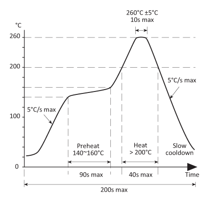
Soldering Profile
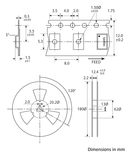
Tape & Reel Specification
Handling & Storage
 Human Body Model (HBM) 1A (250V to <500V)
 Moisture Sensitivity Level (MSL): 1 (or not applicable)
Construction
- Ceramic body with gold-plated pads
- Metal lid, seam sealed
Compliance
Please refer to our DOCUMENTS section for more information.
 Lead-free (< 0.1% by weight )
 RoHS compliant with no exemptions.
 REACH compliant.
 Free of conflict minerals.
 Free from halogens.
 Free from ozone-depleting substances.


