
2 Oct 2015
CHRIS WATTS - CHIEF ENGINEER
Golledge's Chief Engineer Chis Watts explains some of the intricacies of reducing the size of quartz crystal resonator, and what it means for your design. First given as part of a talk to ARMMS RF & Microwave Society, this paper gives both an overview of crystal resonator technology, design calculations, and tips on how to accommodate smaller crystals in your design work.
This white paper is available to download for viewing offline here (no registration required).
Introduction
As with the rest of electronics there has been a move from leaded packages to surface mount and ever smaller packages. While the consequences for this change have been slight for other passive components, crystals do need some design adaptions as the size of the chosen crystal is reduced. The effects of reduced crystal size are described and recommendations for mitigating these effects are discussed.
Size reduction in AT cut crystals
| Product | Size/mm | Year of Introduction | Product image (not actual size) |
|---|---|---|---|
| HC49 | 11.05 x 4.65 x 13.46 | Early 1980s | 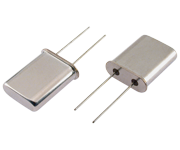 |
| UM1 | 7.8 x 3.2 x 8.0 | Mid 1980s | 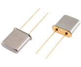 |
| GSX49-4 | 12.9 x 4.8 x 4.3 | 1993 | 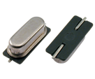 |
| GSX-751 | 7.0 x 5.0 x 1.2 | 2000 | 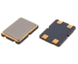 |
| GSX-531 | 5.0 x 3.2 x 0.7 | 2001 |  |
| GSX-431 | 4.0 x 2.5 x 0.8 | 2003 |  |
| GSX-331 | 3.2 x 2.5 x 0.8 | 2004 |  |
| GSX-321 | 2.5 x 2.0 x 0.6 | 2005 |  |
| GSX-221 | 2.0 x 1.6 x 0.55 | 2008 |  |
| GSX-211 | 1.6 x 1.2 x 0.45 | 2012 |  |
Size Reduction in Tuning Forks
| Product | Size/mm | Introduction | Product Image |
|---|---|---|---|
| GWX-26 | 2.1 x 6.2 | Traditional |  |
| CM8V | 2.0 x 1.2 x 0.6 | 2010 |  |
| TBC | 1.6 x 1.0 x 0.38 | In Development | TBC |
The Crystal Electrical Model
24MHz GSX‐331
This model ignores overtone and spurious resonances. Non‐linear effects are also not modelled. The motional resistance (R1) is sometimes referred to as RR. This is not the same as ESR.
ESR = R1 * (1 + (C0/CL) )2

CL is the load capacitance in a parallel resonant mode application.
Effects of Shrinking the Crystal

From HC49 to GSX‐211

Reduced C0
The thickness of the quartz is set by the frequency (a 26MHz AT‐cut fundamental is 64µm thick), so that does not change. The other dimensions of the quartz crystal have to be shrunk to fit the package. This results in smaller electrodes. C0 is proportional to electrode area. An approximate equation is given below. This ignores the effects of fringing and package parasitic capacitance.
C0 = A * Ff * 0.026
C0 is in pF, A is the electrode area in mm2, Ff is the fundamental resonance in MHz
Reduced Motional Capacitance (C1)
The motional capacitance is proportional to electrode area for a given frequency. An approximate expression is given below.
C1 = 0.126 * A * (F/n3)
C1 is in fF, A is the electrode area in mm2, F is the resonant frequency in MHz, n is the overtone.
Trim Sensitivity (TS)
TS = C1 / (2 (C0 + C1)2 )
C1 is the load capacitance
C1 is reduced by changing to a smaller crystal. In parallel resonant applications C0 << CL. Therefore TS is reduced if the application circuit is not adjusted when changing to a smaller crystal.
Motional Resistance (R1)
For a given crystal Q and series resonant frequency, motional resistance is inversely proportional to the active area of the crystal. The active area is about the same as the electrode area. Therefore smaller crystals have a higher R1. In practice the crystal Q for small crystals is not as high as the larger ones. The reduced Q also contributes to a higher R1. If the circuit is not adjusted to accommodate the higher R1 this could result in an oscillator with start‐up problems.
Drive Level Dependency (DLD)
There are many sources and types of DLD. One of particular interest when using very small crystals is a shift in the resonant frequency with changes in the drive level. This is due to nonlinear components in the quartz stiffness. More details of this mechanism can be found in ref[1]. An example can be seen in the plot below. The frequency scale on the right‐hand side shows the series resonance relative to the design parallel resonance. The left hand resistance scale is R1.

Here we see a frequency shift starting to increase at ~20µW. The effect is a function of power density so smaller crystals should be driven with a proportionally lower power. It can also be seen that the motional resistance changes with drive power for the lower frequency crystal indicating a drop in Q if the crystal is over‐driven. The shift in resonant frequency induced by drive level changes adds an AM to PM mechanism that degrades the phase noise performance of the oscillator. The reduced Q also degrades phase noise performance. It is therefore important for optimum phase noise and frequency accuracy performance to avoid overdriving the crystal.
Increased Minimum Frequency
The minimum usable frequency for an AT‐cut crystal of given size is set by the presence of alternative modes of resonance (and their overtones) that interfere with the wanted mode. The alternative modes of resonance can show up as spurious resonances. They can also manifest as “activity dips”. Activity dips are increases in R1 that appear over a narrow temperature range. See ref[2] for more on activity dips. This source also warns of increased coupling into unwanted resonances with increased drive level.
| Package | Package Size (max) | Minimum AT‐cut Frequency |
|---|---|---|
| HC49J | 17.7 x 11.0 x 5.3 | 1.8 MHz |
| UM-1J | 11.6 x 7.8 x 3.6 | 3.579 MHz |
| GSX-751 | 7.0 x 5.0 x 1.2 | 6 MHz |
| GSX-531 | 5.0 x 3.2 x 0.7 | 8 MHz |
| GSX-331 | 3.2 x 2.5 x 0.8 | 10 MHz |
| GSX-321 | 2.5 x 2.0 x 0.6 | 12 MHz |
| GSX-221 | 2.0 x 1.6 x 0.55 | 16 MHz |
| GSX-211 | 1.6 x 1.2 x 0.45 | 24 MHz |
Lower frequencies are available in these small packages by using different crystal cut types that use a different resonant mode. This often comes at the expense of poorer frequency stability. The SL‐cut is an example that uses a face shear vibration mode.
Perturbations
This is a term used to describe a deviation from the ideal frequency V temperature characteristic of the particular crystal cut. These can be caused by the coupling of unwanted modes of resonance as described above. Perturbations can be induced by using a drive power density that is too high.

The measured data in this plot is marked in blue. The red line is the attempt to fit a third order polynomial to the data. For a crystal without perturbations the match between polynomial and measured data should be better than 0.5ppm for all points. A third order polynomial will usually suffice for an AT‐cut crystal.
Package Asymmetry

The move from leaded cans to the modern ceramic surface mount packages means that the stray capacitance between crystal electrodes and package ground is asymmetric. This can lead to small variations in the frequency of an oscillator depending on which way round the crystal is mounted. Care should be taken, particularly when prototyping, that the correct package orientation is used. Note that crystals are characterised with the can (or lid for surface mount types) floating unless stated otherwise. This can also lead to unexpected frequency shifts.
Vibration Resistance
The lower mass of the small surface mount parts is of a benefit when it comes to protection from damage by shock and vibration. The traditional circular crystal blank required three or four point mounting in large packages taking up a large PCB area to avoid damage by vibration or shock. In modern surface mount packages the blank is normally secured by two points of silver‐loaded epoxy that also perform the electrical connection the crystal. Automotive grade surface mount parts have what is referred to as a four point mount of the blank within the package. This consists of two extra points of silver‐loaded epoxy placed on top of the first two after the crystal blank has been placed. The advantage here is that the increased mount rigidity comes without costing any more PCB area. Although this is referred to as four point, the quartz is still only attached by two corners.
Design Changes to Accommodate Smaller Crystals
Reduce Load Capacitance
Reducing the load capacitance has the advantage of maintaining the tuning range of the oscillator. It can also reduce the drive level to the crystal and power consumption of the oscillator circuit. Fortunately the reduction of crystal package size leads to a smaller PCB pad size and therefore lower PCB pad capacitance.
Reduce Drive Level
The drive levels quoted in data sheets are those used for characteristic testing. They may not be the optimum for that part. Characterisation of the crystal should be performed (or ask the supplier for the data) to find the optimum drive level.
How to determine drive level
Drive level can be determined through simulation of the oscillator with the maximum expected value of R1 used in the crystal model. If a realistic model of the behaviour of the active section of the oscillator is not available then the current in the crystal should be measured using a high bandwidth current probe. If you don’t have a current probe then measuring voltage across the crystal can give enough data to derive the crystal drive level. When measuring voltages in this way, care must be taken to avoid loading the circuit with the probe. Ideally the shunt capacitors should be temporarily reduced to compensate for the probe capacitance.